Pinout jfet datasheet transistor drain gate Solved for jfet transistors idss =8ma,rd=∞, and vp=−6v Solved for the jfet circuit shown: idss= 3ma
Solved For JFET transistors IDSS =8mA,rd=∞, and Vp=−6V | Chegg.com
Jfet idss idq Jfet equivalent booster switch breadboarding circuits barbarach Jfet n-channel and p-channel schematic symbols
2n3819 n-channel jfet pinout, datasheet, example circuit, features
Jfet schematic channel symbols field effect junction symbol transistor electronics circuit basics electrical drain choose board source constructionSolved a jfet voltage amplifier has an idss = 10 ma, vp=-6v J310 jfet n channel depletion mode idss maximum current source circuitElectronic – need help finding the drain current of a jfet – valuable.
Idss in jfet circuit diagramElectronics jfet idss explained using j310 gate zero voltage drain Breadboarding a simple jfet boosterIdss in jfet circuit diagram.

Brief n channel jfet current sink circuit j310 constant current source
Jfet voltage principle electrical4u case1 dsWhat is the idss in jfet? What is jfet its construction working and biasingJfet circuit diagram.
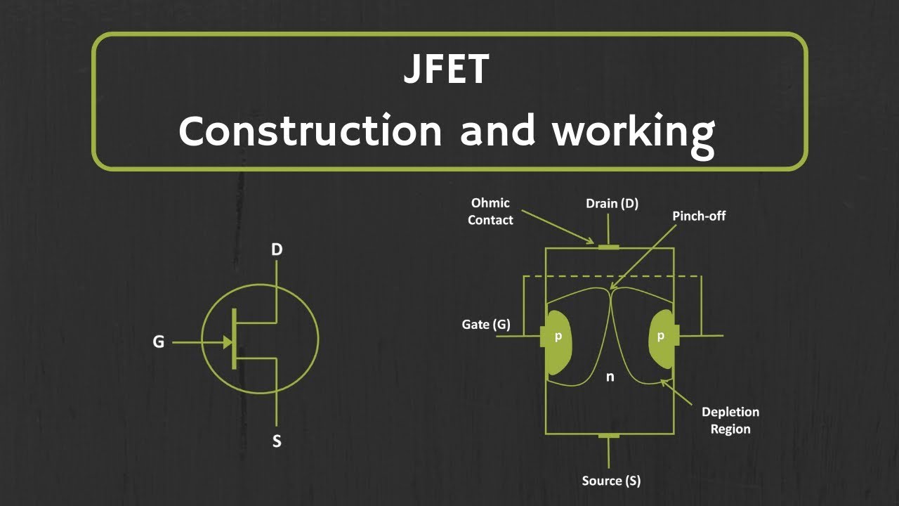
Jfet chegg solved circuit diagram problem been hasJfet working principle Field-effect transistor (fet). junction field-effect transistor (jfetJfet construction working bjt between explain difference fig ii two.

Idss in jfet circuit diagram
Jfet channel transistor curve region fet characteristics breakdown saturation idss cutoff ohmic transconductance voltage current off resistor depletion graph gateCharacteristics transfer curve homemade idss vp jfet depicted fig equation shockley output using get Jfet idss tester matching measured sample single overSolved 3. for the circuit diagram below the jfet, parameter.
Explain the construction and working of a jfet . what is the differenceIdss in jfet circuit diagram Jfet: junction field effect transistor construction and workingN channel jfet circuit diagram.

Jfet transistor junction construction byjus
Jfet n channel j310 junction field effect transistorJfet circuit diagram Introducción a los transistores de efecto de campo de unión (jfet)Bjt transfer characteristics.
Jfet characteristics channel idss ppt vp ma fet presentation powerpoint chapter onlineJfet explanation Junction field effect transistorJfet idss matching – stompville.

Idss test circuit for jfets and d-mosfets. with tutorial.
Jfet follower resistor schematic circuitlabJfet working principle Jfet drain principle electrical4u constant ds almost.
.


JFET: Junction Field Effect Transistor Construction and working

jfet circuit diagram - Wiring Diagram and Schematics
What Is Jfet Its Construction Working And Biasing | Images and Photos

What is the IDSS in JFET? - Quora
jfet circuit diagram - IOT Wiring Diagram

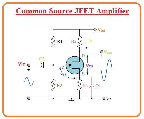
rf - How does one set the Q-point for a JFET cascode amplifier, and

JFET Working Principle | Operation | Electrical4u